General informations
The CABRE tradition
The circuit topology of the AS-202 follows the basic choices already made in other CABRE power amplifiers and which demonstrated their worth.
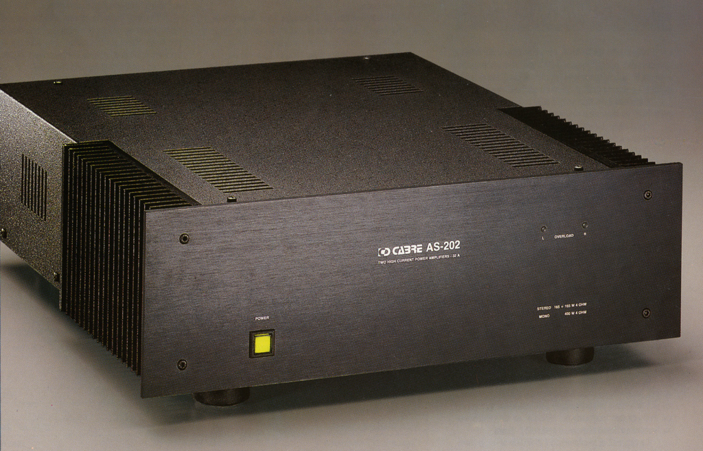
The unit consists of two completely indipendent mono power amplifiers placed in the same box. Such independance offers several advantages, like the absence of dynamic influence between the two channels and a greatly improved reliability in a professional use.
Power stage
A J-FET operational amplifier is placed before the actual power amplification stage, and it can be also used in inverting configuration for mono operation (bridged), thus delivering an amount of output power equal to the sum of power values supplied by each channel.
The circuit is totally complementary symmetry one (all stages symmetrical - input to output).
Each stage features local negative feedback and it has been linearized through sophisticated circuit arrangements. It was therefore possible to charge a low total feedback, with all the resulting advantages concrening stability and sound quality.
The semiconductors employed are the best offered by modern technology as regards specifications directly connected to sound quality as well as reliability. Each channel is equipped with four power transistor (MJ15003/ MJ15004) which are capable of dissipating up to 1 KW altogether and supplying maximum current of 80 A.
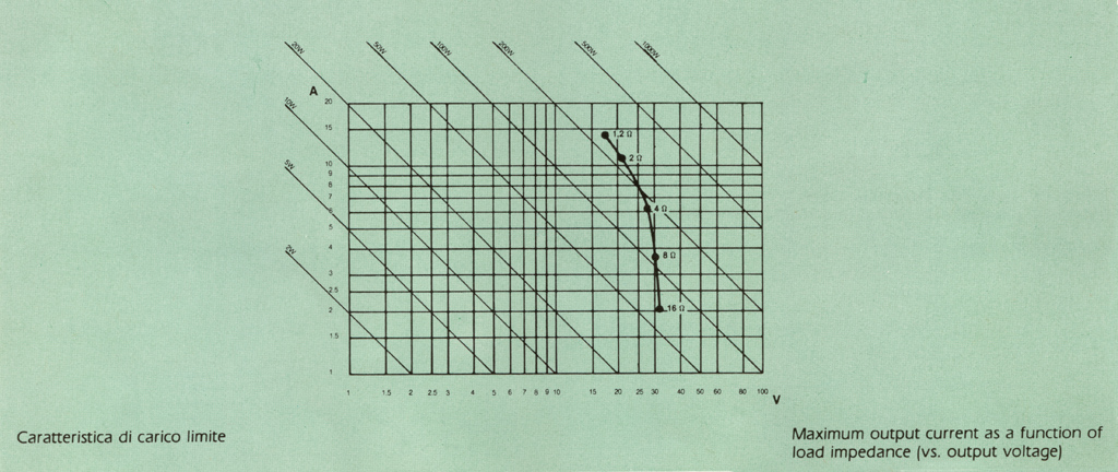
The electronic protection circuit works according to current amount only, and is arranged to operate when peak value goes over 22 A.
Power supply section
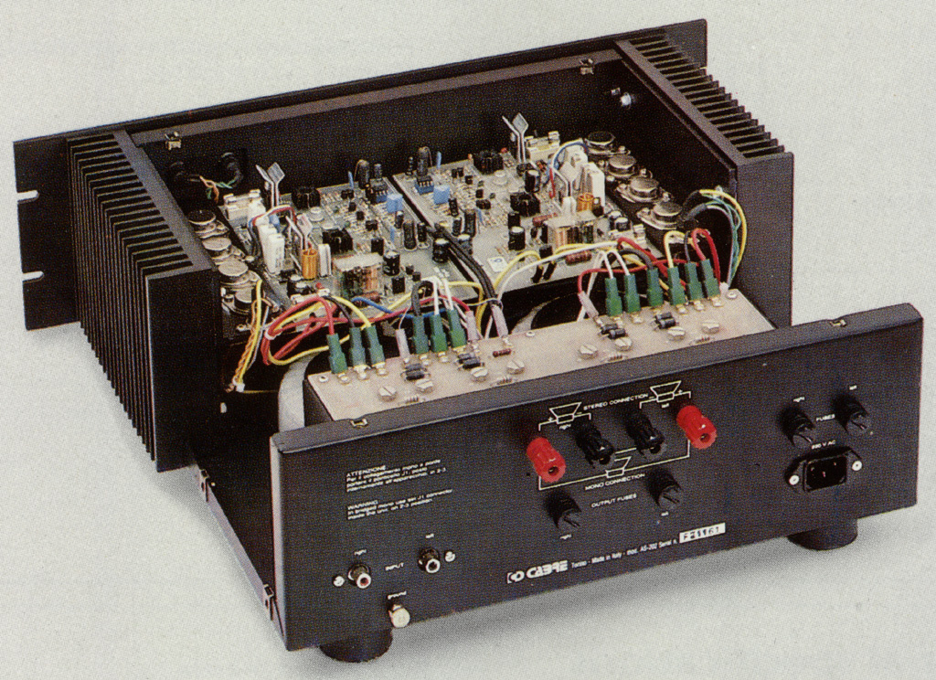
Power supply stage is individual for each channel to avoid any dynamic interference, to ensure high power stability and improvement of stereo image.
This stage features two high efficiency toroidal transformers, of very low disperse flux and considerable power. Levelling capacitance is 40,000 uF and that makes an energy reserve almost twice as much as that normally available in a normal 100+100 W power amplifier.
Technology
The amplification stage is assembled on a glass fibre printed circuit board and placed directly onto the heat-sinking group.
Each power semiconductor has around 600 sq cm heat sinking surface, arranged on different masses with different thermal resistivity.
A differential heat sinking action is thus obtained, optionally operating both in case of thermal peaks and of longer cycles with lower temperature shifts.
Components employed are professionally quality and guarantee great reliability and constant performance in prolonged service life.
|